
A single layer of atoms may seem too thin to meaningfully interact with light, yet materials like tungsten disulfide are reshaping what is possible in nanophotonics. Researchers have now found a way to dramatically strengthen these interactions.
Atomically thin semiconductors such as tungsten disulfide (WS₂) are emerging as key materials for next-generation photonic technologies. Although they consist of just a single layer of atoms, they support tightly bound excitons, which are electron-hole pairs that interact strongly with light. These materials can also produce new colors of light through nonlinear optical effects such as second-harmonic generation. Because of these capabilities, they are considered promising for quantum optics, sensing, and compact on-chip light sources.
However, their atomic-scale thickness also presents a fundamental challenge. With so little material present, light has limited opportunity to interact with it. As a result, light emission and frequency conversion processes are typically weak unless the surrounding optical environment is carefully designed to boost these interactions.
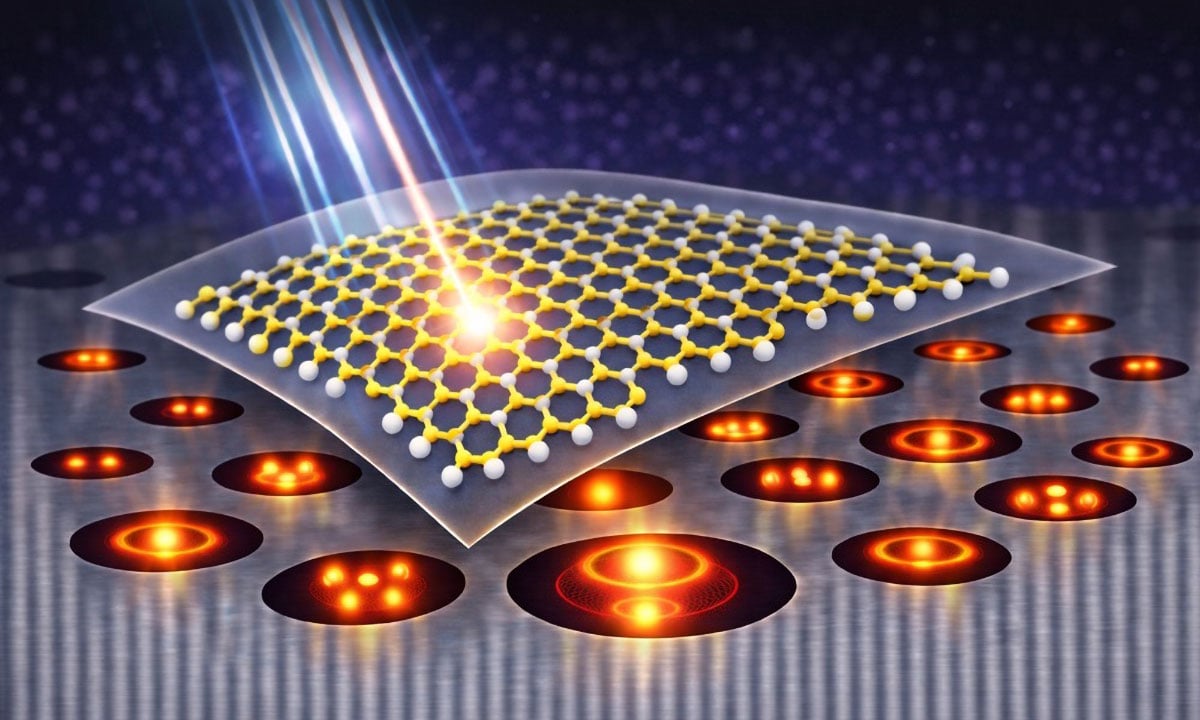
A study published in Advanced Photonics presents a new solution that focuses not on altering the two-dimensional material itself, but on reshaping the structure beneath it. In this work, researchers created a hybrid system in which a monolayer of WS₂ rests on nanoscale air cavities known as Mie voids. These voids are etched into a high-index crystal of bismuth telluride (Bi₂Te₃). The team demonstrated that this configuration significantly strengthens both light emission and nonlinear optical signals, while also making it possible to directly observe localized optical modes.
Turning empty space into a resonator
Traditional dielectric nanoresonators confine light within solid materials such as silicon. While this method can be effective, it tends to concentrate optical fields inside the bulk of the material rather than near its surface, where atomically thin layers are located. In addition, if the host material absorbs light, resonances become damped and the field intensity drops.
Mie voids rely on a different concept. Instead of trapping light inside a solid structure, they confine it within tiny air cavities carved into a material that has a very high refractive index. Strong reflections at the air-dielectric interface keep light circulating inside the cavity. This arrangement concentrates the optical field within the air space and close to the cavity opening, precisely where a monolayer placed on top can interact with it most effectively.
This inverted confinement strategy provides several benefits. The enhanced field is directly accessible to materials located at the surface. The resonant wavelength can be tuned by adjusting the cavity dimensions. The design also remains effective even when the surrounding material absorbs light strongly. Bi₂Te₃, which is not ideal for conventional solid resonators, performs well in this void-based architecture.
Designing and fabricating the heterostructure
Using full-wave electromagnetic simulations, the researchers engineered cavities that support a simple dipolar resonance matched to the primary emission feature of WS₂, known as the A-exciton. By modifying the radius and depth of each cavity, they were able to control both the resonance wavelength and the vertical location of the optical mode within the structure.
The team fabricated the voids by focused ion beam milling into thick, mechanically exfoliated Bi₂Te₃ flakes. Each cavity was positioned far enough from its neighbors to behave as an independent resonator rather than as part of a coupled array. A continuous WS₂ monolayer was then transferred over the patterned surface. This single sheet covered resonant cavities, non-resonant cavities, and flat substrate areas. Because the same monolayer spanned all regions, any differences in optical response could be traced to cavity geometry instead of variations in material quality or illumination conditions.
Optical reflection measurements confirmed the design predictions. Larger cavities produced a steady shift of the resonance toward longer wavelengths. Changing the cavity depth while keeping the radius constant caused additional spectral shifts and gradually moved the optical mode deeper into the structure. Even when the geometry deviated from the optimal design, the resonances remained clearly defined, demonstrating strong tolerance to fabrication imperfections.
Enhancing light emission from WS₂
To evaluate how the cavities influence light emission, the researchers measured photoluminescence from WS₂ while varying the depth of the voids under laser excitation. When the cavity resonance overlapped with the WS₂ emission band, the photoluminescence intensity increased by roughly twentyfold compared with the most detuned cavity.
Simulations indicated that there was no meaningful field enhancement at the excitation wavelength. Additional measurements using different pump wavelengths showed that maximum emission consistently occurred at the same cavity depth. These findings ruled out enhanced absorption of the incoming light as the main explanation. Instead, the improvement arises from emission-related effects. The resonant cavity increases the local optical density of states and enhances the efficiency with which emitted light escapes.
Because the WS₂ layer was continuous across the entire sample, the team could directly compare light emission from resonant cavities, non-resonant cavities, and flat regions under identical experimental conditions. This direct comparison confirmed that the contrast in emission was driven by resonance engineering rather than differences in the monolayer itself.
Probing nonlinear optics and visualizing modes
The researchers also adapted the cavity dimensions to shift the dipolar resonance into the near-infrared range. Under resonant pumping, the second-harmonic signal from WS₂ increased by about twenty-five times compared with non-resonant cavities. As the pump wavelength was tuned across the cavity resonance, the signal displayed a pronounced spectral peak.
In addition to boosting signal strength, the platform allows direct spatial imaging of localized optical modes. Far-field images of the second-harmonic emission showed bright, well-defined hotspots positioned above individual voids. When the pump wavelength or cavity depth was adjusted, these hotspots shifted across the array in a predictable pattern that reflected the designed dispersion of the resonant modes. This approach provides a real-space view of how optical fields evolve within individual resonators, without requiring specialized near-field probes.
A flexible platform for atom-thin photonics
By integrating tunable optical enhancement with precise spatial control in a van der Waals compatible structure, Mie-void heterostructures offer a versatile way to work with atomically thin materials. The design avoids the need for large periodic metasurfaces and remains effective even in materials that strongly absorb light, which are typically challenging for conventional photonic devices.
This platform could enable advances in nonlinear light generation, surface-enhanced sensing, and spatially programmable photonic systems built from two-dimensional semiconductors. More broadly, the study shows that shaping empty space can be just as important as selecting the right material when designing nanoscale light-matter interactions.
Reference: “Light–matter interaction in van der Waals heterostructures with Mie voids” by Zhuoyuan Lu, Kirill L. Koshelev, Pavel Tonkaev, Ziyu Chen, Dawei Liu, Wenkai Yang, Yuri Kivshar and Yuerui Lu, 14 February 2026, Advanced Photonics.
DOI: 10.1117/1.AP.8.2.026002
Never miss a breakthrough: Join the SciTechDaily newsletter.
Follow us on Google and Google News.
Source link
-

-

-

-

-


