Defect-filled lead-halide perovskites rival silicon solar cells because domain walls inside the material separate and guide charges. Researchers visualized these charge-transport networks using a novel silver-staining technique, resolving a long-standing efficiency mystery.
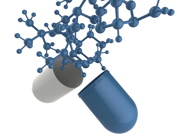
Perovskites made from lead halides are produced through low-cost solution processing and contain many defects. Even so, they convert sunlight into electricity with efficiencies close to those of silicon cells, which remain the commercial benchmark. In a study published in Nature Communications, physicists at the Institute of Science and Technology Austria (ISTA) report a detailed physical explanation for this surprising performance.
For years, scientists have wondered how a material made with relatively simple, inexpensive methods could rival silicon technology refined over decades. Over the past 15 years, lead-halide perovskites have rapidly emerged as promising candidates for next-generation solar cells. Unlike silicon, which requires extremely pure single-crystal wafers, perovskite devices can be fabricated using affordable solution-based techniques while still delivering comparable results.
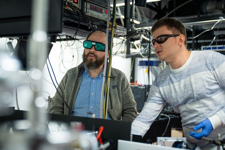
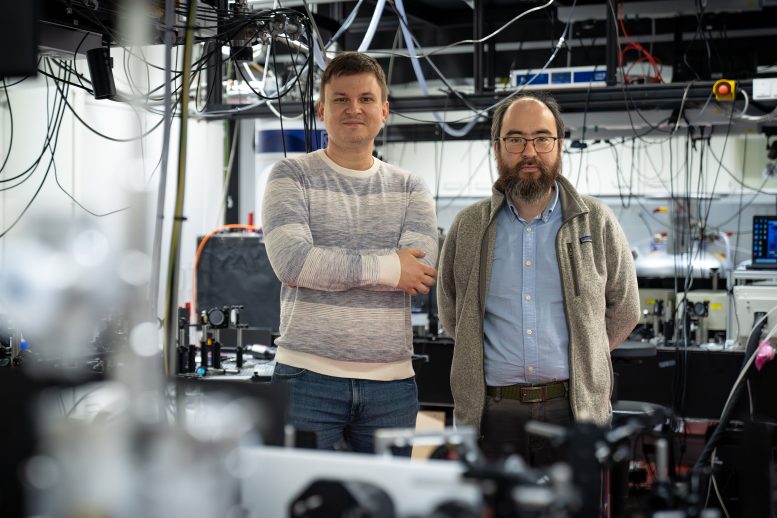
Postdoc Dmytro Rak and assistant professor Zhanybek Alpichshev at ISTA have now identified the mechanism behind these unusual photovoltaic properties. Their research shows that, whereas silicon depends on near-perfect purity to function efficiently, perovskites actually benefit from their internal imperfections. A dense network of structural defects enables electric charges to travel long distances through the material, which is essential for efficient solar energy conversion.

“Our work provides the first physical explanation of these materials while accounting for most–if not all–of their documented properties,” says Rak. The results could accelerate the transition of next-generation perovskite-based solar cells from the lab to real-world applications.
From Obscure Compounds to Quantum Materials
The term “lead-halide perovskites” refers to a family of compounds first identified in the 1970s. They were named because their crystal structure resembles that of perovskites, a well-known class of oxide materials widely studied in materials science. Aside from their ability to form stable hybrid organic–inorganic crystalline structures, these compounds initially attracted little attention and were largely set aside after basic characterization.
Interest surged in the early 2010s when researchers discovered their remarkable ability to convert sunlight into electricity. Beyond solar cells, perovskites have proven useful in LEDs and X-ray detection and imaging. “In addition, these materials exhibit astounding quantum properties, such as quantum coherence at room temperature,” explains Alpichshev, whose group studies complex phenomena in condensed matter systems.
To generate electricity, a solar cell must first absorb light and create charge carriers: negatively charged electrons and positively charged “holes.” These charges must then travel to the electrodes, where they are collected as electric current. The difficulty lies in the journey. Charges must move across distances of hundreds of microns, which is comparable to hundreds of kilometers on a human scale, without being trapped.
In silicon devices, this challenge is addressed by minimizing defects that could capture charges before they reach the electrodes. Perovskites, by contrast, are full of such imperfections because of how they are made. This raises a key question: how do charges manage to move so far in a material that appears so disordered? And why do they survive long enough to be collected?
Excitons, Internal Forces, and Charge Separation
Experiments have shown that when electrons and holes bind together in perovskites to form an exciton, they tend to recombine quickly. Yet measurements also indicate that separated charges can persist for surprisingly long times. To explain this contradiction, the ISTA team proposed that internal forces within the material must be pulling newly formed electron-hole pairs apart, preventing them from recombining.


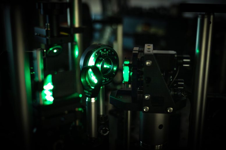
To investigate, the researchers used nonlinear optical techniques to generate electrons and holes deep within a perovskite crystal. Each time they created a new group of charges, they detected a measurable current flowing in the same direction, even without applying an external voltage. “This observation clearly indicated that even deep inside single crystals of unmodified, as-grown perovskites, there are internal forces that separate opposite charges,” says Alpichshev.
Earlier studies had suggested that such behavior should not occur based on the known crystal structure. To resolve this inconsistency, the team proposed that charge separation happens in specific regions rather than uniformly throughout the material. These regions, known as domain walls, are areas where the crystal structure is slightly altered and can form interconnected networks across the sample.
Confirming the presence of these domain walls deep inside the crystal posed another challenge, since most measurement techniques probe only the surface. Surface properties can differ significantly from those in the interior.
Visualizing Domain Walls and Charge Highways
Rak approached the problem from a chemical perspective. Because perovskites conduct ions as well as electrons, he reasoned that introducing special marker ions might reveal the location of domain walls without damaging the material. He developed an electrochemical staining method in which silver ions diffuse into the crystal and preferentially gather at domain walls.
The silver ions were then converted into metallic silver, making the domain-wall network visible under a microscope throughout the entire thickness of the crystal. “This qualitative technique, invented and implemented at ISTA, is much like angiography in living tissues—except that we are examining the micro-structure of a crystal,” says Alpichshev.
According to Rak, realizing that a natural network of charge-separating domain walls densely spans the entire bulk of perovskites was a game-changer. As he explains, “If an electron-hole pair is created near a domain wall, the local electric field pulls the electron and the hole apart, placing them on opposite sides of the wall. Unable to recombine immediately, they can drift along the domain walls for what seems like eons on a charge carrier’s timescale and travel long distances.”
The researchers describe these interconnected domain walls as “highways for charge carriers.” They provide a clear explanation for the exceptional charge transport that underpins the strong performance of perovskite solar cells.
Implications for Next-Generation Solar Cells
The team emphasizes that this work delivers the first unified physical framework that accounts for the many unusual properties observed in lead-halide perovskites. “With this comprehensive picture, we are finally able to reconcile many previously conflicting observations about lead-halide perovskites, resolving a long-standing debate about the source of their superior energy-harvesting efficiency,” says Rak.
Until now, most efforts to improve perovskites have focused on adjusting their chemical composition, often with limited gains. The new findings suggest that engineering and optimizing domain-wall networks could enhance performance while preserving the inexpensive manufacturing methods that make these materials so attractive for future solar technologies.
Reference: “Flexoelectric domain walls enable charge separation and transport in cubic perovskites” by Dmytro Rak, Dusan Lorenc, Daniel M. Balazs, Ayan A. Zhumekenov, Osman M. Bakr and Zhanybek Alpichshev, 16 February 2026, Nature Communications.
DOI: 10.1038/s41467-026-68660-5
This research was supported by the Scientific Service Units (SSU) of ISTA through resources provided by the Imaging & Optics Facility (IOF) and the Miba Machine Shop Facility (MS).
Never miss a breakthrough: Join the SciTechDaily newsletter.
Follow us on Google and Google News.
Source link